
Updated 7/6/09 (see dated updates below)
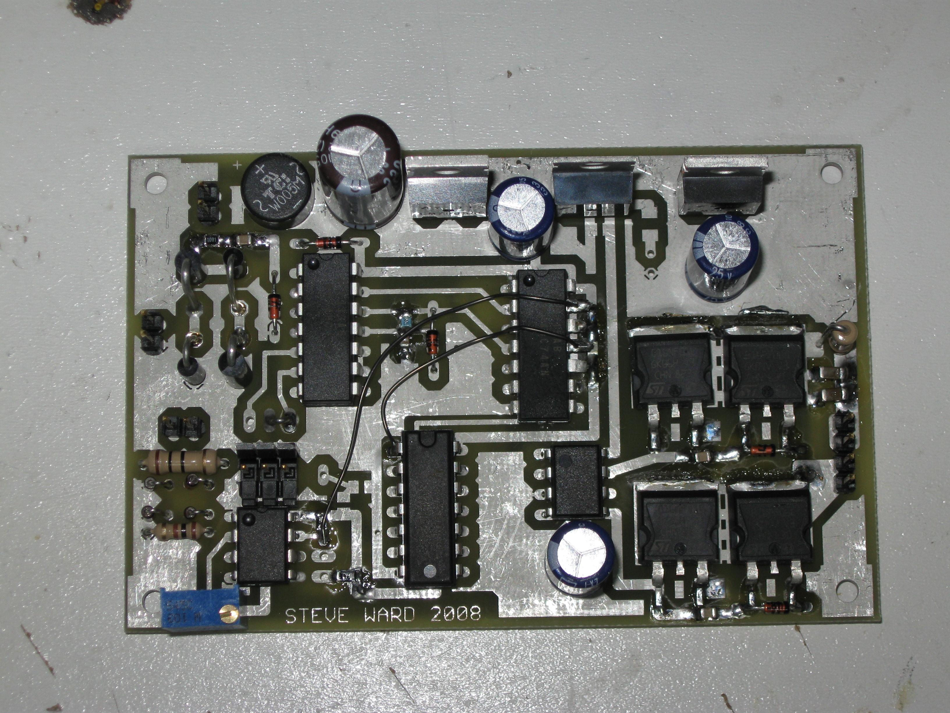
Having built a few DRSSTC drivers using IGBT bricks, I realized what a pain it was to build the large gate driver circuit I had previously developed. In search of something simpler, I turned back to our old friend the Gate Drive Transformer (GDT). I used to believe that it was not possible to drive large CM IGBT modules with a GDT, but I proved myself wrong. There are a few important details that must be done properly to get good results from a GDT drive. They are:
Note, the original design (including PCB) have been modified. The files listed here reflect these changes. Please see further down this page for the newer design files.
PDF schematic of driver/controller (error fixed 6/25/09)
EAGLE board file (right click, "save as")
Bottom Component Placement (pdf)
This driver is very similar to my other ones, with a few important exceptions. The gate driver section is now very robust, using 16A P/N mosfet pairs. The input to the gate driver is set at 24VDC, so that a 1:1 GDT ratio can be used and still achieve 24V on the IGBT gate. I no longer believe its necessary to drive the gates to 30V unless you are absolutely pushing the IGBT to the extreme. Otherwise, the higher gate drive voltage just makes the possibility of gate oxide failure more likely. Even with 24V drive, TVS diodes should be placed right at the IGBT gate terminals to clamp the voltage to less than 30V.
In order to support the new gate drive setup, some additional logic was required, and was provided with a quad AND gate. I also switched over to the 74HC74 D-Flip Flop instead of the 74HC109 JK flip flop, because its 14 pins instead of 16. I also used some hacks to replace the 555 astable timer with just an RC on the input to an AND gate, in the overcurrent detection circuitry.
Another example of this driver in use can be seen here. This coil uses a full-bridge of 40N60 mini-bricks from fairchild semi. The tank cap is a pair of special CDE caps, each rated 100nF at 8kVDC (estimated VAC rating of 2kV). The GDT was wound with cat-5e network wire, using the "white" conductors as the primaries (4 in parallel) and the other 4 wires as secondaries. A 5.1 ohm gate resistance is used, and is bypassed on the discharging edge with a 1n5819 diode. The primary is tuned low to 170khz. This coil is a solid performer producing up to 38" sparks with only an 11" long secondary winding.
IMPORTANT: The over-current detection comparator has a limited operating voltage range for its inputs. When operating from 5V, as in this circuit, the trip level set by the potentiometer should NOT exceed 3.75V for reliable operation. Setting it above this voltage may completely disable the OCD functionality. Lower the burden resistance (on the ODC input) if this is a problem.
A note on using fiber optic receiver OPF2412:
This one seems to come back and haunt me from time to time. Im using the OPTEK OPF2412 fiber optic receiver. These are noise sensitive devices, and not surprisingly, problems show up when I use them around tesla coils. Firstly, they really should be in a metal enclosure. Secondly (and quite surprisingly), the metal sheath that is at the end of the ST fiber cable should be bonded to the metal box. It may seem absurd that a small piece of metal just a few millimeters from the lens of the Rx would be able to effect the thing, but surely enough it does. The issue is either that this metal ring picks up some RF and couples it into the Rx, or its simply that the metal ring, when grounded, extends the electrostatic shielding of the Rx. Im gonna go with number 2. Anyway, the fix for me was to just put a small steel spring that presses against the box and the ST end when its plugged in. It may be wise to stick all of the low voltage electronics into a metal box too. One more odd problem discovered and solved!
UPDATE 11/23/2008 (some of this may not make sense as i have removed the original schematics):
There were a few quirks with this design that i wanted to correct. The RC circuit for the current limiter was fussy and hard to get working just how i wanted, also it turns out the difference between HCT and HC logic made a big difference in the circuit performance. So i present an updated schematic that is a much more robust design. Terry Blake gave me the inspiration for using the extra D flip flop to set the "disabled" state of the controller. Operation is simple, when the comparator senses a trip condition, its output drops low, causing the D flip flop to clear its output, which disables the interrupter pulse via the AND gate. The controller stays in the disabled state until a rising edge from the next interrupter pulse puts the D-FF back high. This also has the added benefit of keeping the indicator LED ON for the maximum permissible amount of time (rather than just 1mS or something). Below is a updated schematic that documents the surgery necessary for my PCB design.
Also, the BOM is probably a tad outdated. Most of the important parts are there (all the ICs and caps) but it may be lacking a resistor or 2 or something like that. I suggest you check over the new schematic before trusting the BOM solely.
Id also like to report that this driver is now used on my revised edition of the DRSSTC-0.5. It works great even at 300kHz! Truly a universal driver.
UPDATE 2/11/09:
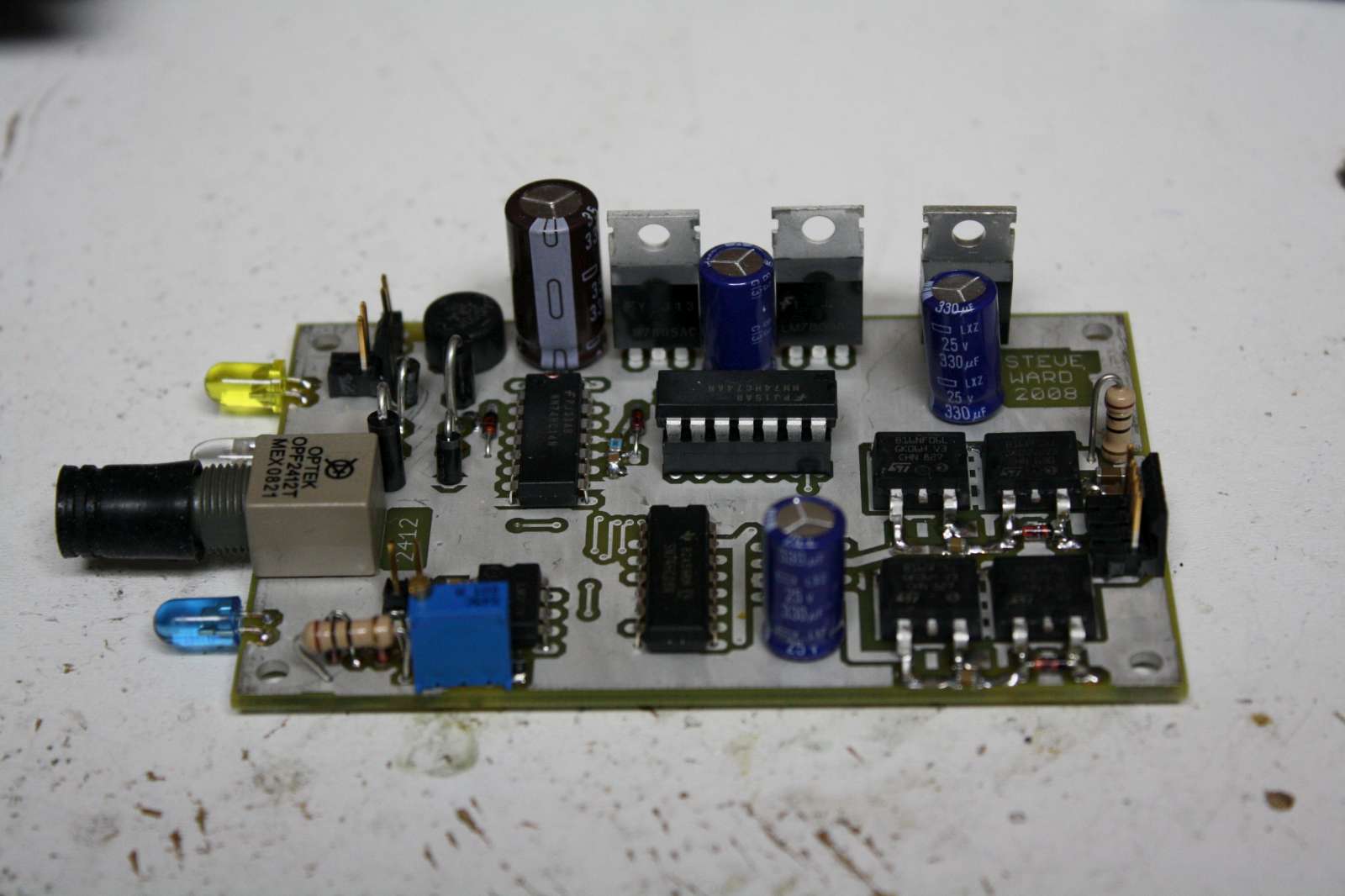
I have re-spun the PCB for this driver. The main reason was that I wanted to put the fiber optic receiver on the PCB, and also because i modified the over-current detection inhibit circuitry. Below are some helpful files for this new board. Another afterthought modification to this design deals with the current sensing circuitry. Having the burden resistance (R5) before the bridge rectifier (D8-11) and having yet more burden resistance (R4) after the bridge, made it less than straight forward to pre-determine the volts-to-amps scaling of the circuit. So now the burden resistance is moved to be only after the bridge rectifier, and to handle the larger currents, I suggest using 1n5819 schottky diodes instead of the 1n4148 signal diodes. Furthermore, the somewhat large .1uF filter cap on the sensing input to the LM311 comparator was causing other scaling errors (its a significantly low impedance at 100khz) so I've changed it to 1nF, or I find it can be left off altogether.
Schematic 1.3b (error fixed 6/25/09)
Board file 1.3 (.brd)
Top Component Placement (pdf)
Bottom Component Placement (pdf)
A mostly complete Parts List (.xls) (updated 7/6/09)
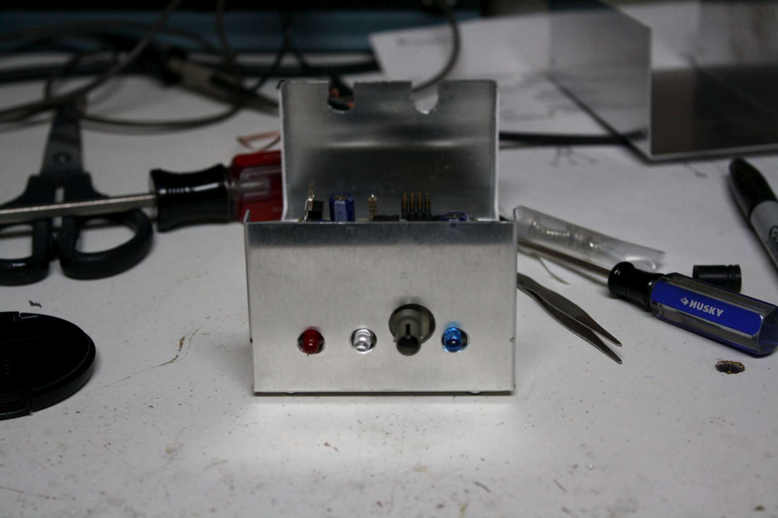
Pictures of the new board:

UPDATE 6/25/09:
While analyzing something with this driver, I realized the schematics were drawn incorrectly, the inputs to the UCC27423 dual gate driver were swapped. Updated schematics have been posted. This is a minor error that shouldn't impact any design significantly.