The HVSSTC
Page created: 12/10/03
For the most part it seems that SSTCs have run into a spot where sparks of more than 24" or so are difficult to achieve. Dan McCauley experimented with using a MOT as a SSTC power supply. I looked into this extensively but there is just one HUGE problem with series MOSFETs needed to switch some 2500VDC. Pspice simulations displayed for me just how bad the problem was. I simulated a half-bridge design with 6 IRFP460 FETs per leg. Adding just 30ns (that's not much!!) of delay on one of the FETs caused the voltage across it to raise to well over 1kv. This of course being the whole problem with series FETs... timing.
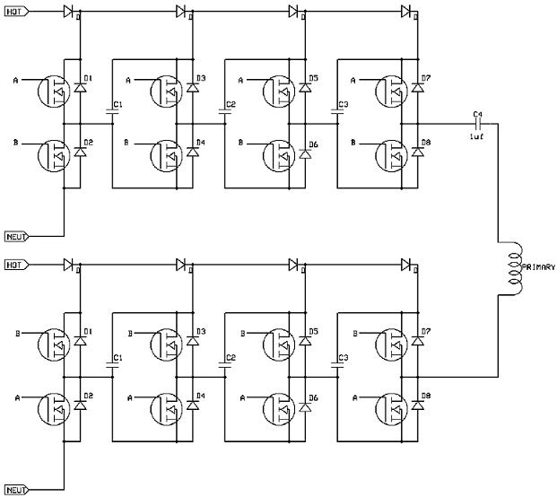
Well, a friend from the 4HV. group (Dan Strother) showed me a new topology that was actually posted on the TCML quite awhile ago. This is the document which started it all. Look at the bottom of page 51. You will see a multi-level inverter topology with self-balancing. Now we take this and make it SSTC worthy!
(NOTE: I forgot to add the decoupling capacitors across the power supply input in the schematic.)
Its a lot to take in at once. Basically we have two 4-level inverters. Each level consists of one half-bridge producing an RMS voltage of 1/2 the input voltage (just like any half-bridge). This means that each 4 level-inverter is producing 2X the input voltage. Now, notice the gate indicators A and B and how the top inverter is opposite the bottom. The 2 inverters will produce 4X the input voltage in their current configuration.
EXPLANATION OF OPERATION:
It took me awhile to see just how this topology works. Lets simply focus on one of the inverters. There are 2 conditions: 1) the top FETs are on and the lower FETs are off, 2) the opposite of that. When the top FETs are off the lower FETs allow the mains input to charge the capacitors C1-C3 to the supply voltage through the diodes at the top. All caps are charged now to 340V for instance in my case. Now, the top FETs turn on. The first half-bridge now outputs 170V into the base of C1 raising the potential of the second half-bridge by 170VDC. Then this bridge also pushes on the next, but its already at 170V potential so it pushes C2's base up to 340V. This half-bridge then acts on the final half-bridge making its output 510V and so on. So the 4 level inverter is putting out 680V when the top FETs are on (basically all of the supply capacitors are in series, like in a Marx generator). Now, when the lower FETs turn back on we now see the return path to ground (neutral). Thus we now have high voltage output from our low voltage MOSFETs! The 2 inverters working together (in opposition) will give 1360V across the primary (that's 2720V peak to peak!!).
Now, there are of course some drawbacks to this design. The first is that the lower left-hand MOSFET will have to conduct the full supply current since it is supplying the current that charges the capacitors. Each of the following lower FETs see less and less current (as they are supplying current to less stages). This is not much problem when you have 500V 80Arms rated MOSFETs ;o). The top MOSFETs see the same current that will be produced across the primary coil (maybe 2-3A average at 1360V). So the top FETs have an easy life. So my basic setup will have the first 2 half-bridges made of 80N50s and the last 2 bridges made of 48N50s and likewise for the second inverter. I do not want to mix MOSFETs in the same bridge as that could cause problems with timing within the half-bridge modules (i.e., shoot-through problems).
Now the beauty of this circuit! Timing delays between stages don't matter! At least not in the sense of a series MOSFET switch. In fact this inverter was designed to have different stages on at different time periods to simulate stepped sine waves at the output (refer back to the linked PDF file). Simulations in pspice suggest that no single fet will ever see more than the voltage supply input even when things are severely out of synch. Though, timing is important due to the fact that the freewheeling diodes will see uneven currents on the delayed stages. Chances are I will only have about 30-40ns delays at most between stages. I'm using 30A ultra-fast diodes so there should not be much problem here.
As we look, we see that the MOSFETs towards the output of the inverters see less and less current. There are already future plans to add on additional stages of IRFP460 MOSFETs to perhaps get some 2-3kv across the primary if the results of this initial design look promising!
Final note: C1-C3s are for now planned to be 5uf but this may change as I see how it acts in real life testing.
UPDATE: 1/14/04
I wired up a new primary on an 8" sonotube form using 12awg wire. So far I've been using the 17 turn tap with sparks up to about 24" now. The secondary is the large 6.625"x24" winding of 28awg with a 12"x1.5" toroid. Moving the coil closer to the feedback board helped with the problems I was having before. Here are some pictures from this test run:
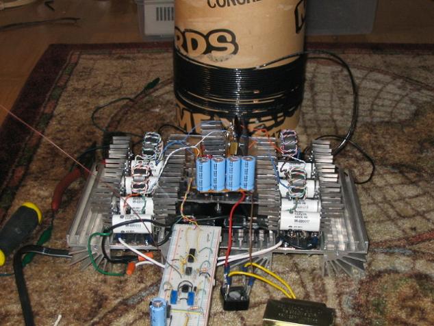
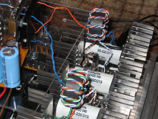
Here are some still shots from the video I took:
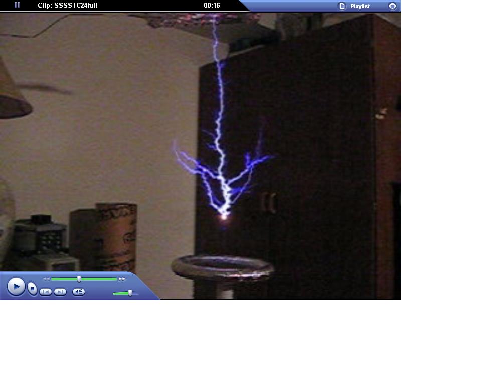
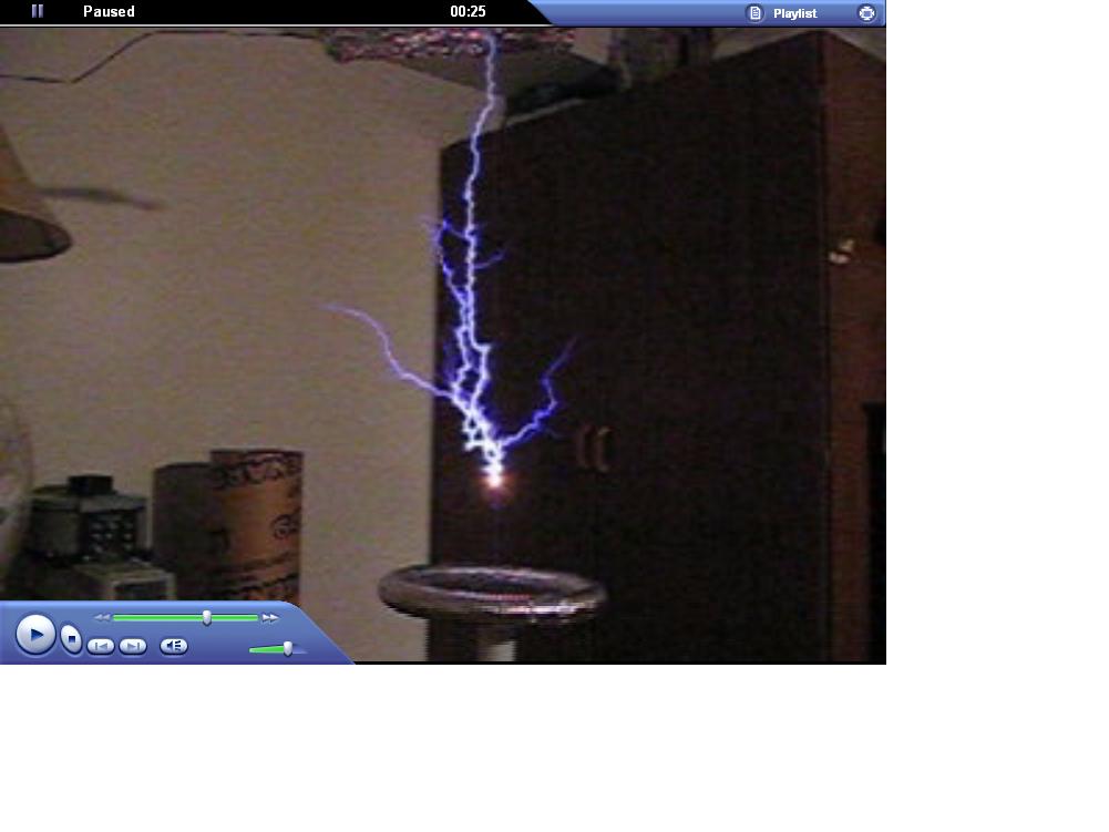
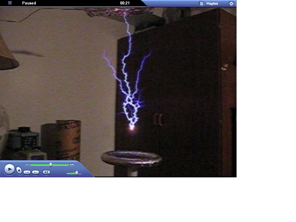
Things are getting exciting ;-)
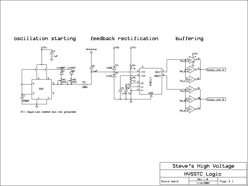
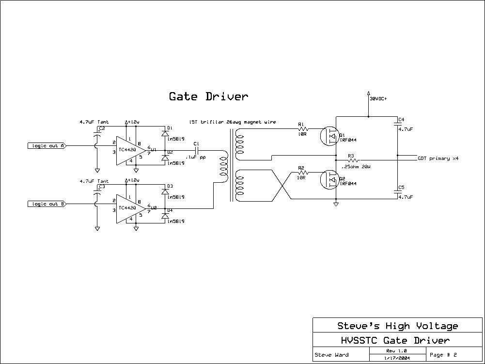
Here are the schematics for the feedback and gate driver sections of the SSTC.
More Updates (3/27/04):
I made a big decision to reduce the number of MOSFETs in this design to 8 FETs. Why you ask? Well, to save money (those big FETs are expensive!), also, I don't think I need such a high voltage. I now basically have two 2-stage inverters. So at a full 400VDC peak input I should see 800VDC peak, or 1600V peak to peak. This should still be plenty as its 2X what an h-bridge could do. So now I'm driving only 8 FETs, the gate waves look much better, about 200ns rise times, rail to rail. Initial testing up to 140VAC input and 11 primary turns looked to be producing about 24" sparks. The fact that its using 11 primary turns instead of say, 4 or 5 is promising. I then recently wired up my 240V variac. Things were looking great up to about 160VAC input, where I had 2 MOSFETs fail! After talking with Jimmy H. for a bit, we drew the conclusion that it was most likely an over voltage failure. When they failed, one fet had 200ohms resistance from D-S, and the other 30ohms... they did not blow dead short like most FETs do. From what I read, this is a sign of exceeding the devices avalanche ratings (normally avalanche rated devices will withstand over voltage up until a certain energy level). So, logically, I replaced the bad FETs and its working again. I began scoping the D-S voltage on each fet, and at 80VDC input at 4A into a resistive load, everything looks perfect. Each fet sees the voltage supply, no more. So the actual failure is rather mysterious to me, the only thing I can think of to do is add some TVS across them (the TVSs are on they way ;-)).
Final Update:
Project ended, DRSSTCs put this topology to shame for this application, no need to put any more effort into this project.